
Project introduction
Project introduction

Wafer slicing is an essential process in semiconductor chip manufacturing process, which is the last process in wafer manufacturing.
The splitting of a finished wafer into individual chips (grains) based on the size of the chip is called a wafer slicing.
The rapid development of optoelectronics industry in recent years.
The demand for high integration and high performance semiconductor wafers is increasing.
Silicon, silicon carbide, sapphire, glass and indium phosphide are widely used as substrate materials for semiconductor wafers.
With the increase of wafer integration, wafers tend to be thin and light, and many traditional processing methods are no longer applicable.
Therefore, laser stealth cutting technology is introduced in some processes.
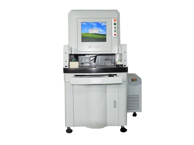
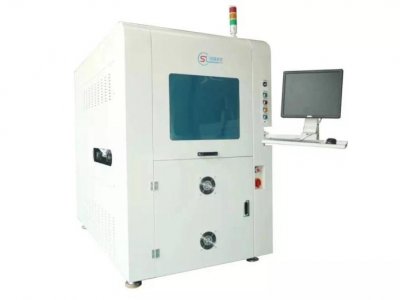
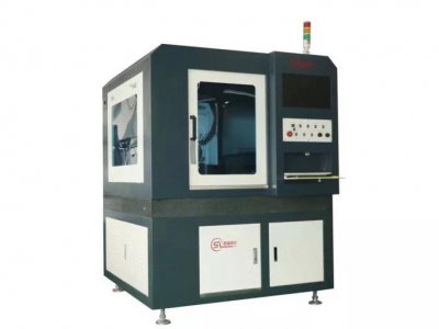
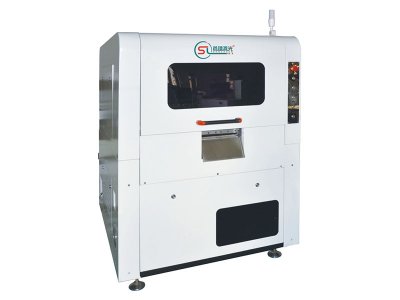
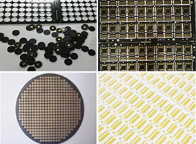
Related products
Laser stealth cutting technology for semiconductor wafers is a new laser cutting technology. Its main principle is to focus the short pulse laser beam through the material surface in the middle of the material, in the middle of the material to form a layer, and then apply external pressure to separate the chip.
Cost analysis
Cost analysis
Picosecond laser, customized focusing head, focusing beam diameter to 3 m, cutting path only 10 m, narrow slit, more chip out rate, no thermal effect, no damage to the chip circuit.
The scribing speed is up to 500mm/s. For samples with a thickness of less than 1mm, the laser scribing can be broken only once.
CCD visual prescan & automatic target positioning, maximum processing range 650mm×450mm, and Mosaic accuracy of XY platform ≤±3 m.
No taper cut, minimum edge collapse 3 m, smooth edge.
Supports a variety of visual positioning features, such as crosses, solid circles, hollow circles, L-shaped right-angle edges, image feature points, etc.
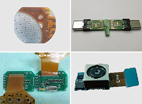
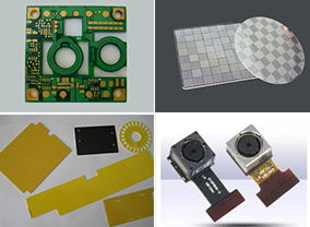
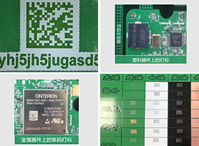
Application cases
Applications


 Jiangsu Headquarters:NO.600 Dong Ding Road, Ba ChengTown Kunshan City, Jiangsu Province